 Physics (Internal)
Experimental Condensed Matter Physics
Rama Bansil, Keith Brown, Scott Bunch, Michael El-Batanouny, Wanzheng Hu, Maria Kamenetska, Karl Ludwig, Raj Mohanty, Kevin Smith, Alexander Sushkov, Anna Swan, Ophelia Tsui, M. Selim Ünlü, Alice White
Condensed matter experiments examine the structure and behavior of condensed states of matter where interactions between adjacent atoms, molecules, and electrons determine the physical nature of the material. Condensed matter physics occupies a unique niche in physics. Developments in this field are often of equal importance for technological applications and for improving our fundamental understanding of the nature of matter. One need only consider the revolution caused by the development of the transistor, and a similar one likely to follow from the discovery of high-temperature superconductors.
Boston University continues its rapid growth in condensed-matter physics with strong research efforts in photonics, scattering physics, surface physics, advanced materials physics, low-dimensional electronic systems, low-temperature physics, and structural biology and chemistry. Condensed matter experimentalists in the Physics Department are also playing major roles in the University's Photonics Research Center and Center for Nanoscience and Nanobiotechnology. In these efforts, as well as many others, condensed matter experimentalists work in close association with scientists in the College of Engineering.
Research
- Applications of Nanomechanical Devices: Wireless Communications and Sensors
Our research in this specific area focuses on the development of ultra-high-frequency (UHF) oscillators, filters and frequency-selective elements for eventual use as high-speed sensors and communication systems. Our systems are nanomechanical oscillators, and they vibrate at speeds exceeding 2 GHz—the highest mechanical frequency ever reported. Because of their mechanical construct and the small size, they will enable a host of future applications. Currently, we are exploring specific applications, which include nanomechanical memory elements for high-speed high-density data storage and gigahertz-range nanomechanical oscillators for use as frequency-selecting device in cellular phones.
- Dynamics of Polymer Nanometer Films
It has been broadly observed that the physical properties of polymers, including the elastic modulus, freezing temperature and relaxation behaviors, can become quite different from the bulk when the the material is molded into a nanometer film or structure. Recently, our group developed a method that has enabled us to measure the viscosity of polymer nanometer films with thicknesses from 2 to above 100 nm. In this method, we monitor the dynamics of the height fluctuations of the films and model it with the dynamics of surface capillary waves, which is related to the flow property and hence effective viscosity of the films. Through these measurements, we have made illuminating observations about the rich influences of the interfaces and confinement effect - namely the effect of confining the polymer chains in a dimension smaller than the unperturbed radius of gyration. Having a good understanding of these influences is essential to effective usage of polymers in nanoscale applications.
- Experimental Studies of Gels
Rama Bansil’s primary interest is in gels, which are found in numerous products of daily use, have fascinating visco-elastic properties, fundamentally different than solids or liquids. Bansil’s laboratory is devoted to interdisciplinary research ranging from Polymer Physics to Biophysics. Through a variety of experimental methods such as light scattering, small-angle X-ray and neutron scattering, and microscopy complemented by computer simulations of model gels, Bansil’s group has elucidated the structure of gels at the molecular level, the physics of gel formation, diffusion in gels and the kinetics of phase transitions and chemical reactions in gels. Current research projects include the phase behavior of multiblock copolymer gels and their application to develop templates for nanoscale devices. Many living tissues are in the form of gels, which has excited a great deal of interest as a substrate for tissue regeneration. Bansil and her collaborators at Harvard Medical School have focused their attention on understanding the role that gelation of mucin (a glycoprotein found in the mucus layer) plays in preventing the stomach from being digested by the highly acidic gastric juice that it secretes. Their studies using dynamic light scattering and atomic force microscopy have contributed to a detailed mechanism of how mucin molecules gel under acidic conditions.
- Experimental Surface Physics
Elastic and inelastic scattering of neutral thermal beams of helium atoms or metastable 3S helium atons are used to study the dynamical and magnetic properties of surfaces.
The surface physics group at Boston University has been one of the pioneers in neutral helium atom scattering from solid surfaces in the mid 1980s, and our facility is one of seven worldwide. The technique is the surface equivalent of thermal neutron scattering from bulk crystals, which has provided valuable information about bulk dynamics and structural phase transitions over the past three decades.
Helium atomic scattering was used by our group to study the structural and dynamical evolution during the initial growth of ultra-thin metallic composite films. These investigations have impact on the understanding of basic physical phenomena, especially non-linear physics, as well as potential technological applications. For instance, most cutting-edge technologies involve thin-film growth processes in the synthesis of artificial materials, such as the surface modification processes in the fabrication of electronic and magnetic devices.
Another direction of investigations using helium scattering were recent studies of the dynamics of hydrogen atoms on metallic surfaces have led to the discovery of the surface quantum motion of hydrogen, thus shattering the conventional perception of localized hydrogen atomic bonds.
The surface physics group at Boston University has pioneered, in the 1990, a novel technique that employs spin-polarized metastable helium atoms to investigate, for the first time, the long-range magnetic (or spin) ordering on surfaces of a class of crystalline materials known as antiferromagnets. In this class of materials the net magnetization is zero, but the direction of the spins alternate from one direction at some site to the opposite direction at neighboring sites. Many of the new high Tc materials belong to this class. The studies provide valuable information about how changes in the atomic environment at the surface modify the long-range order of the spin structure. The technique probes whether all the surface electronic spins point in a single direction (ferromagnetic), are randomly oriented (non-magnetic), or exhibit a more complex spin ordering than observed in the crystalline bulk. It also has the capability of providing detailed information about propagating surface magnetic (or spin) waves, such as relations between their frequencies and wavewlength. The effort is backed by large-scale computer simulations used to model dynamical and magnetic properties of surfaces, and thus provide detailed information about the microscopic mechanisms.
One of the interesting results obtained with this technique, revealed the unique behavior that on the crystalline surface of CoO, the degree of magnetic-ordering increases with temperature over the range 250K to 320K!
- High Resolution 4Pi Microscopy
Confocal fluorescence microscopy has developed into a standard tool in cell biology research; Light can easily penetrate inside the cell and furthermore, a fluorescent dye can be made to interact with specific cellular components, for example attach to an antibody that binds to a cellular protein. The resolution of confocal microscopy is ca 0.5 um laterally and 0.75 um axially.
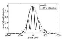
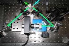
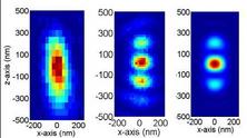
The axial resolution of a conventional confocal microscope can be improved by a factor of 3-5 in 4Pi microscopy. A 4Pi confocal fluorescence microscope uses two opposing, high numerical aperture objectives, shown in Fig 1. The counter propagating wave fronts of the illumination form interference fringes at the common focal point of the two objectives. Likewise, the collected light is interfered at the detector. This effectively reduces the axial focal volume compared to conventional confocal microscope, illustrated in Fig. 2. The measured point spread function for a fluorescent 100 nm bead is shown in figure 3. The improvement in axial resolution using two objectives (b) compared to standard confocal microscopy (1) can clearly be seen.
We are now combining 4Pi microscopy with an interferometric method we have developed, spectral self-interference fluorescent microscopy. The technique transforms the variation in emission intensity for different path lengths used in fluorescence interferometry to a variation in the intensity for different wavelengths in emission, encoding the high-resolution information in the emission spectrum. Using monolayers of streptavidin, we have demonstrated better than 5nm axial height determination for thin layers of fluorophores and built successful models that accurately fit the data.
- Microring Resonator Biosensors
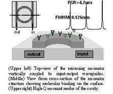 Microring resonators provide high sensitive label-free optical biosensor platforms. The light coupled into the resonator via a waveguide is confined within the microring cavity due to total internal reflections and high-Q resonant modes (Q~12000) are formed. The positions of these modes depend on the effective index of the resonant structure and thus get shifted when there is a molecular interaction on the surface. This shift can be determined with high precision using our method of detection. We have accomplished to demonstrate biosensing application of the microring resonators by investigating a well studied binding event (Avidin-Biotin complex). The high sensitivities (1.8×10⁻⁵ refractive index units) obtained with this method are comparable to commercially available surface plasmon resonance devices.
The detection methods that are currently available deliver high sensitivity and specificity; however they fail to provide a clear path to compact optical packaging that will lead to portable devices for field use. Towards this goal, and with the efforts of our interdisciplinary research team and industrial collaborators, we are currently modifying our table-top, fiber-coupled system to develop a cost- efficient, compact integrated biosensor platform.
Microring resonators provide high sensitive label-free optical biosensor platforms. The light coupled into the resonator via a waveguide is confined within the microring cavity due to total internal reflections and high-Q resonant modes (Q~12000) are formed. The positions of these modes depend on the effective index of the resonant structure and thus get shifted when there is a molecular interaction on the surface. This shift can be determined with high precision using our method of detection. We have accomplished to demonstrate biosensing application of the microring resonators by investigating a well studied binding event (Avidin-Biotin complex). The high sensitivities (1.8×10⁻⁵ refractive index units) obtained with this method are comparable to commercially available surface plasmon resonance devices.
The detection methods that are currently available deliver high sensitivity and specificity; however they fail to provide a clear path to compact optical packaging that will lead to portable devices for field use. Towards this goal, and with the efforts of our interdisciplinary research team and industrial collaborators, we are currently modifying our table-top, fiber-coupled system to develop a cost- efficient, compact integrated biosensor platform.
- Novel Materials Laboratory
The goal of this research program is to understand experimentally how electronic structure determines the optical, electrical, magnetic, structural, and chemical properties of new and unusual materials. A powerful array of electron and photon spectroscopic probes is used to measure electronic structure. Some of these probes are well established, while the development of others is an exciting and important component of our research efforts. This is an ambitious interdisciplinary program that combines elements of physics, chemistry, and materials science, and addresses issues of fundamental scientific and technical importance.
The spectroscopies used in our studies are soft x-ray emission, resonant inelastic x-ray scattering, soft x-ray absorption, angle-resolved photoemission, and core level x-ray photoemission. All of our experiments are performed off-campus at synchrotron radiation light sources. We presently run experiments at
i) the National Synchrotron Light Source, Brookhaven National Laboratory in New York,
ii) the Advanced Light Source at Lawrence Berkeley National Laboratory in California, and
iii) the MAXLAB synchrotron in Lund, Sweden.Currently, five distinct classes of materials are under investigation: low-dimensional and correlated solids, organic metals and semiconductors, III-N nitride semiconductors, transparent conducting oxides, and rare-earth nitrides. Each of these independently funded projects is described below.
1. Many Body Physics in Low- Dimensional and Correlated Solids
Correlated and low dimensional solids present important challenges to modern solid-state physics. While our knowledge of the origin the physical properties of many simple solids is both comprehensive and sophisticated, this is not the case in low dimensional and correlated solids. From quasi-low dimensional conductors, through magnetoresistive oxides, to high temperature superconductors, there exists a plethora of physical phenomena displayed by these materials that remain poorly understood. Transition metal oxide bronzes are inorganic quasi-low dimensional correlated solids that are ideal prototypical systems for spectroscopic studies, due to the large size and high quality of available crystals. Among the unusual properties of these oxides are low-dimensional electron transport, metal-insulator and metal-metal transitions, periodic lattice distortions and charge-density-wave transport. Many of these phenomena are related to the coupling between vibrational modes of the lattice with the electrons at the Fermi level. Of particular importance in this coupling is the structure of the Fermi surface itself. Despite its fundamental role, the structure of the Fermi surface in low-dimensional systems is generally undetermined. Our research program addresses numerous aspects of the physical nature of these oxides and combines the information on each topic into a coherent model for their low dimensional properties. We measure quasi-low-dimensional Fermi surfaces, metal d-band dispersion, spatial localization and hybridization of the d-electrons, bonding interactions at different sites in the lattice, the creation of energy gaps at the Fermi level, and the formation and structure of point and extended defects.
2. Organic Semiconductors and Metals
Organic electronic materials are of interest due to both the technological promise of carbon-based devices and to the scientific challenge posed by these materials to our understanding of basic physical processes in complex solids. Despite the importance of semiconducting organic materials, there have been few studies of their valence band electronic structure using modern synchrotron radiation-based spectroscopic methods. In part this is due to the difficulty in preparing clean samples for study, but also due to the severe x-ray radiation beam damage suffered by these materials. We are undertaking a comprehensive synchrotron radiation-based soft x-ray spectroscopic study of a variety of thin film organic electronic materials, including semiconductors, metals, and molecular magnets. The organic films are grown in-situ, with proper attention paid to minimizing beam damage effects. The films are grown in a custom built organic molecular beam epitaxy chamber attached to the spectrometer chamber at a soft x-ray undulator beamline at the National Synchrotron Light Source. Information is obtained on the element and site specific valence band partial density of states, band dispersions, chemical state, and orbital bonding in the films. Our work on novel organic metals is undertaken in collaboration with Professor Linda Doerrer in the BU Department of Chemistry, whose group synthesizes the materials.
3. III-Nitride Semiconductors
Our third area of research concerns the surface and interface properties of nitride semiconductors. GaN and related III-V nitrides (InN, AlN) are candidates for use in high-temperature microelectronic devices and used in blue wavelength light-emitting diodes and lasers. Despite success in the growth and application of these materials, the basic physics underlying the intentional doping of the films, the nature of defects, and the formation of metal overlayers remains to be determined. All of these problems are related directly to the detailed electronic structure of the nitrides, and yet this structure has not been extensively measured. The development of these nitrides as electronic materials requires that their defect and dopant electronic structure be fully understood. In collaboration with Prof. Ted Moustakas from the BU College of Engineering, we undertake a comprehensive determination of the detailed electronic structure of thin film refractory nitrides. Specifically, the electronic structure of defects and dopants in these nitrides is being studied, as well as the electronic structure of the interface between the films and their substrates, and between the films and metal overlayers. Furthermore, the chemical reactivity of the films (in particular, when defective or doped) is being investigated in order to understand the nature of adhesion of these nitrides to both substrates and overlayers, and to understand the chemical stability of the films at elevated temperatures or in model corrosive environments.
4. Transparent Conducting Oxides
Transparent conducting oxides (TCOs) play a crucial role in thin film solar cells. Central to the operation of such cells is the ability to have solar radiation penetrate the cell and be absorbed, with the light efficiently converted to an electrical current that can be extracted. To accomplish this in thin film solar cells, the outer body of the cell needs to be optically transparent yet electrically conducting. TCOs are the enabling technology in this regard. There is an inherent competition between optical transparency and electrical conductivity, and great efforts are being expended to achieve low resistivity TCOs that can be doped reproducibly both n-type or p-type. Since the interest in TCOs lies in their electronic properties, a comprehensive study of their electronic structure is of vital importance in understanding the properties of these materials, improving their synthesis, and discovering new TCOs. We are measuring the detailed surface and bulk electronic structure of novel TCOs using our set of complimentary synchrotron radiation-based soft x-ray spectroscopies. The TCOs are synthesized by Professor Russ Egdell, from the Department of Chemistry, Oxford University. Our measurements hold the promise of significant impact in the area of TCOs for use in solar energy conversion.
5. Rare-Earth Nitrides
The rare-earth nitrides form a closely related family of magnetic semiconducting or semimetallic materials, exhibiting interesting properties because of the strongly correlated 4f electrons. We use our array of spectroscopic techniques to measure the electronic structure of rare-earth nitride thin films grown in-situ, as well as films capped with suitable protective layers grown by our collaborators in New Zealand: Professors Joe Trodahl and Ben Ruck from Victoria University. The spectroscopies provide unique and complementary information on the energy position, splitting and degree of hybridisation with other states of the occupied and empty 4f- states. Resonant inelastic x-ray scattering provides additional insights into the excited states of the 4f system and into other many-body effects related to these strongly correlated electrons. Calculations of the electronic structure are undertaken using the LSDA+U approach (local spin-density approximation complemented with orbital dependent Coulomb and exchange interactions) and implemented in the full-potential linear muffin-tin orbital method by Professor Walter Lambrecht from Case Western Reserve University. Calculations of the spectroscopic quantities are being developed to extract the maximum information from the experiments. The theoretical analysis of the spectra will identify the need for theoretical developments beyond the mean-field approximation embodied by current LSDA+U, such as integrating atomic multiplet splitting theory with band structure approaches and dynamic mean field theory. Furthermore, calculations of optical conductivity from interband transitions are carried out and correlated with measurements of the same quantity from the infrared to the near UV to be carried out by the NZ group. The calculations also tie the electronic structure to magnetic properties by calculation of the magnetic exchange parameters.
- Numerical Aperture Increasing Lens Microscopy (NAIL)
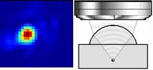
Numerical Aperture Increasing Lens (NAIL) microscopy is a far-field subsurface imaging technique that simultaneously enhances the light gathering power and resolution of an optical microscope. When a NAIL is placed on the backside of a sample, its convex surface effectively transforms the NAIL and the planar sample into an integrated solid immersion lens, capable of aberration-free imaging of the structures underneath the substrate. Addition of the NAIL to a standard microscope increases the numerical aperture (NA) by a factor of the square of the optical index n. The NAIL technology has had the greatest impact in the field of optical failure analysis of Si integrated circuits. In silicon, the NA is increased by a factor of 13. Using an optimized confocal microscope, we have already demonstrated a lateral resolution of 230 nm. Recently, we have applied the technique to optical spectroscopy of single quantum dots demonstrating an 8-fold improvement in light collection from a single dot.
- Quantum Computing: Quantum Control of Coherence of the Electron Wave Function
This project involves the development of quantum control techniques to externally control coherence properties of electron wave functions, or to increase the coherence time of electron wave functions in sub-micron and nanoscale mesoscopic systems. The main thrust behind our approach is to develop enabling technologies for increasing the coherence time scales from the usual nanosecond range to microseconds or even milliseconds. The long-term direction is to perform picosecond time-domain reflectometry and a host of quantum control techniques (open-loop, closed-loop learning feedback and bang-bang).
- Quantum Nanomechanics: Quantum Motion to Testing the Limit of Quantum Mechanics
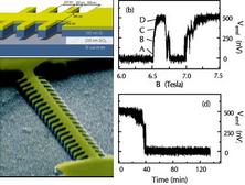
Our current research efforts in this area involve the observation of quantized displacement, energy quantization and Rabi oscillations in macroscopic mechanical oscillators. We have already observed the first two phenomena. In the next few years, we will explore approaches to use these mechanical systems as quantum bits, particularly for quantum information processing. Furthermore, we are exploring foundations of quantum mechanics with these experiments, which involve the largest quantum systems ever realized in a laboratory.
- Quantum sensing using NV centers in diamond
We use nitrogen-vacancy (NV) centers in diamond to perform magnetic imaging on the nanometer scale and study the fundamentals of statistical mechanics and many-body physics of interacting spin systems. Visit my website for more details.
- Real-Time X-Ray Studies of Materials Processes
Our research investigates how materials evolve on atomic and nano- length scales during growth, patterning or electrochemical function using real-time x-ray techniques. Many of the experiments use the high brightness of synchrotron x-ray sources – the National Synchrotron Light Source (NSLS-II) at Brookhaven National Laboratory on Long Island and the Advanced Photon Source (APS) at Argonne National Laboratory outside of Chicago. Where possible, our research makes contact with fundamental theory and simulation.

In the last few years, our detailed interest has been in understanding surface and thin film processes. Many of our in-situ studies utilize a unique ultra-high vacuum growth and surface modification facility that we have helped develop at the NSLS-II. We have been using it to examine surface morphology evolution during ion bombardment (which can cause the spontaneous growth of surface nanostructures) and issues related to the growth of wide-bandgap group III-V semiconductor films using atomic layer epitaxy (in collaboration with the Eddy group at the Naval Research Laboratory).
Increasingly our experiments utilize coherent x-ray scattering, which provides the ability to probe nanoscale dynamics during growth and patterening. Partially coherent x-ray beams are created using small (few microns) slits in conjunction with a high-brilliance 3rd generation synchrotron source. The disorder on the surface produces speckle patterns in the scattered x-ray intensity. The evolution of the speckle pattern can then be related to the underlying dynamics of structural changes.
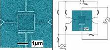
- Resonant Cavity Imaging Biosensor (RCIB)
The Resonant Cavity Imaging Biosensor (RCIB) detects binding between target biomolecules from a sample and probe biomolecules fixed to a microarray surface with the potential for tens of thousands of simultaneous parallel observation sites. Such ability yields information about the affinity of the biomolecules under test for the molecules on the capturing surface. Information about the affinity between molecules of interest such as particular proteins or DNA strands, yields great benefit to a number of applications in biological research, medical diagnostics, and biohazard detection. Current high-throughput microarray technology requires that the target molecules be labeled with a fluorescent dye. At best, this preparation step adds an acceptably small amount of time and money, but at its worse, can be prohibitively difficult depending on the nature of the application.
RCIB operates label-free without the need to add fluorescent labels or otherwise modify the target molecules in any way. An optical IR beam couples resonantly through a cavity constructed from Bragg mirrors that contains the microarray surface; the wavelength of the IR beam is swept using a tunable IR laser source; and an IR camera monitors cavity transmittance at each pixel, creating a highly parallel signature of transmittance versus wavelength for the microarray surface. This novel technique is enabled by high quality silicon substrates with buried Bragg reflectors previously developed within our group for improved photodetectors. The technique additionally relies on the use of commercial telecommunications hardware that has become readily available in recent years. In an alternative approach for microarray detection, the reflection from the substrate is measured with the varying wavelength. When binding occurs on the surface of the wafer, reflectivity vs. wavelength curve shifts, from which the height information can be extracted. This alternative approach is less sensitive than RCIB, but it draws attention with its simplicity. RCIB improves on existing label-free methods by offering dramatically improved throughput necessary to meet the needs of the microarray user community.
- Spintronics: Control of Spins with Nanomechanical Torque

Our current research efforts in this area involve a new proposal for spintronics: spin detection and control can be done mechanical torque. We have recently proposed a comprehensive technique to carry out a series of experiments for demonstrating spin current and spin transfer across a hybrid junction of nanowire, fabricated on top of a two-element suspended torsion oscillator with sub-micron features. The proposed plan of this 3-year project is to demonstrate spin detection and control. This project involves measurement of single-spin conductance and the value of Planck’s constant.