==========================================================================
Reference:
- Previously Microcontroller lab 2 and Microcontroller lab 3, written by Dan Gastler (dgastler@bu.edu) and Eric Hazen (hazen@bu.edu) from BU EDF
- MCP4921 DAC datasheet
===========================================================================
In this lab you’re going to learn about digital-to-analog conversion and timer interrupts. Digital-to-analog conversion is essentially the process of converting a numeric value (usually binary) to an electrical signal. The device which accomplishes this is called a DAC. DACs are widely used in many applications, including the generation of audio signals in digital music players.
Required reading:
PWM
http://arduino.cc/en/Tutorial/PWM
Lab 3.1: Using the PWM DAC
The Arduino has a simple built-in DAC (digital-to-analog converter) which uses the technique of pulse-width modulation (PWM). Please read the brief tutorial on PWM if you haven’t.
Build a pulse width modulation DAC:
- Wire an LED between Arduino pin 3 and GND. Use resistors as needed to limit current.
- Write a sketch which calls analogWrite() to pin 3 with various values from 0 to 255.
What happens to the brightness of the LED? Connect an oscilloscope to pin 3. You should see a train of pulses. What is the frequency?
Make a table in your notebook with 3 columns as follows:
| PWM Value | Pulse Width | Voltage (for 3.2) |
| 0 | ||
| 64 | ||
| 128 | ||
| 192 | ||
| 255 |
Set the PWM to each of the values suggested and measure the pulse width.
Often it is useful to get a programmable DC voltage from a PWM signal, you can use a low-pass filter to convert the pulse train to a DC value (see 3.2 below)
Lab 3.2
Design a low-pass RC filter with a cutoff frequency which you think is appropriate to get a DC value from the pulse train. Test it. If you still see pulses, the frequency is too high. Experiment with different R, C until the output is smooth (less than maybe 100mV of ripple) What component values did you end up with? What is the cutoff frequency?
Fill in the third column of the table with your filter connected (use a volt meter).
The filter you have designed is a common feature of systems which generate waveforms from digital data (like mp3 players).
Limitations of PWM — PWM works well applications where speed is not important (such as dimming LEDs or controlling motor speed). It is not so good for generating waveforms.
Lab 3.3
Measure the maximum frequency you can output with your filtered PWM DAC
With the oscilloscope connected to the output of your filter, enter and run the following sketch:
——————————
int d = 1; // half-cycle delay in ms
void setup() { }
void loop() {
analogWrite( 3, 0); // set PWM to minimum
delay( d);
analogWrite( 3, 255); // set PWM to maximum
delay( d);
}
—————————–
This sketch will output a square wave (in principle) with a frequency of 1/2d where d is the delay for one half-cycle in ms.
Lab 3.4 Using the Serial DAC
To overcome the speed limitations of PWM, we can use an external DAC.
The DAC we will use for this lab is the Microchip MCP4921 (link to data sheet).
Please open the data sheet and skim at least pages 1-2 and 17-25.
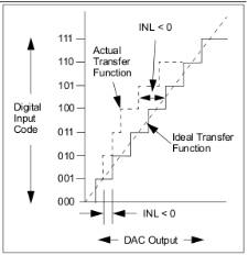
The MCP4921 is a 12-bit serial converter with an SPI bus interface. It accepts a 12-bit binary number (decimal values 0-4095) and converts it to a voltage from 0-5V (with normal gain settings). The graph below illustrates the transfer function of a typical DAC.
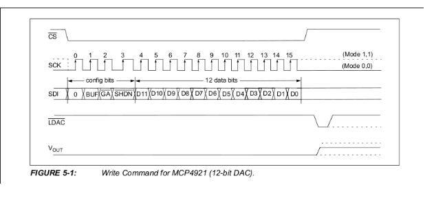
To communicate with the DAC you must use a specific protocol called SPI. To quote page 23 of the data sheet:
“The write command is initiated by driving the CS* pin low, followed by clocking the four Configuration bits and the 12 data bits into the SDI pin on the rising edge of SCK. The CS* pin is then raised, causing the data to be latched into the DAC’s input register.”
Pin Connections
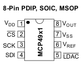
For a data sheet, this is actually quite a clear explanation! Let’s translate it. First, looking at the pinout of the chip below, identify the pins you need:
SDI – DAC pin 4 to Arduino pin 11
SCK – DAC pin 3 to Arduino pin 13
CS* – DAC pin 2 to Arduino pin 10
You will need to connect those pins to digital pins on your Arduino so you can control them. I suggest using the connections above (for reasons we’ll get to later).
You also need to connect some other pins. First, where is the ground pin?! Microchip has confused us by naming it VSS. This name has historical significance (based on the name of the source terminal of a FET). How would you figure out it is actually GND? A good clue is on page 3 of the data sheet under the ELECTRICAL CHARACTERISTICS table where it says:
“Unless otherwise indicated, VDD=5V, VSS=0V”. So, connect those pins too:
VDD – pin 1 +5V
VSS – pin 7 0V (GND)
Finally, what about the other pins? You can often figure out what to do with them by reading the “PIN DESCRIPTIONS” section. See page 17 of the data sheet. For LDAC it says “This pin can be tied to low (VSS)…” so let’s do that. VREF provides the full-scale voltage and as they suggest it may be tied to VDD (5V). So now we have:
LDAC* – pin 5 GND
VREF – pin 6 +5V
▢ Wire the DAC as given above to your Arduino and the breadboard.
Be sure you connect all the pins somewhere (pin 8, as output, should go to a volt meter/scope)
Make sure that a GND pin on the Arduino is connected to breadboard ground.
Serial Protocol
Now we need to figure out what signals to put on the digital pins to send information to the DAC. See the figure below from page 25 of the datasheet. Be careful; there are figures for a few different parts on this page, and we want the one for the MCP4921.
This diagram tells us that we need the following sequence of operations to load a value into the DAC:
- Initialize (in setup()) by setting nCS to HIGH and SCK to LOW.
We don’t have to worry about nLDAC as we have tied it to GND - Set nCS to LOW
- For bits 15 to 0 (loop):
- Output data (0 or 1) on SDI
- Set SCK to HIGH
- Set SCK to LOW
- Set nCS to HIGH
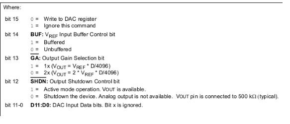
Note that in step 3 you need to provide 16 different bit values. The first four (BUF, GA* and SHDN*) are described on page 24 of the data sheet:
Reasonable choices for these bits would be:
bit 15 = 0
bit 14 = 1 (this is unimportant)
bit 13 = 1 (set output scale to 0-5V)
bit 12 = 1 (enable the output)
Note that the bits with bars over their name are “active low” meaning the named function is active when the bit is set to 0 or “low”. When typing we usually write nSHDN or SHDN*.
So, to set the DAC you would need to send the bits 0, 1, 1, 1 given above followed by twelve bits representing the desired output voltage.
Now you need to write a sketch for the Arduino which produces the signals above. Let’s start with CS*:
int dac_nCS = 10; // pin number for nCS
void setup() { // setup function runs once
pinMode( dac_nCS, OUTPUT); // define nCS as an output
}
void loop() {
digitalWrite( dac_nCS, 0); // set nCS to 0 (LOW)
digitalWrite( dac_nCS, 1); // set nCS to 1 (HIGH)
}
Connect your oscilloscope to the nCS pin.
Check if you can see the CS* pin switching on and off rapidly. A pin value of ‘1’ is indicated by a high level on the diagram. Now you need to make the other signals switch on and off in the order given above. You will add the code to do that between the two digitalWrite() calls which turn nCS on and off.
To do:
Write a sketch to set the DAC to 2.5V
Follow the diagram in Figure 5-1 above.
At first, output the fixed binary value 1000 0000 0000 to the DAC.
This should result in a voltage of 2.5V on the output (pin 8).
Lab 3.5
Write and debug a sketch to output a ramp from 0-5V on the DAC.
Use your oscilloscope as needed to debug it if it doesn’t work.
Here are a few programming hints:
- use the following to test a binary bit in an integer value:
int n; // integer value
int b; // bit number i.e. 0-15
if( n & (1<<b)) // test if bit b is ‘1’ in n
…do something - use a for() loop to output the 12 bits of data
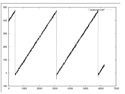
The scope output should look like the plot below, with a peak-to-peak amplitude of 5V. Using my sketch, the frequency is about 10Hz, but yours may be different.
Lab 3.6
Convert the main part of your sketch into a function (Read about Arduino functions if you need review).
Use this function declaration as a prototype:
void setDac( word v)
The function argument v is declared as a word because it is specified to hold a 16-bit value, rather than an int whose size is not specified.
Test your function by writing a sketch which outputs various values to the DAC in succession, and viewing the output on the oscilloscope.
Lab 3.7
Make a new version of the sketch using the Arduino SPI library (reading link).
This requires several changes to your code. First you must add:
#include <SPI.h>
at the top of the sketch to include the function declarations for the library.
Next, you must add:
SPI.begin();
SPI.setBitOrder( MSBFIRST);
to your setup() function. The first line initializes the library. The second tells the library to output the MSB (most-significant bit) first as shown in the timing diagram from the datasheet. Finally, you have to call the function:
SPI.transfer( data);
for each byte (8 bits) to be sent. Note that the DAC requires two bytes (16 bits) to be sent so you have to call the function twice for each update of the DAC. Also note that the library does not take care of the nCS signal, so you need to handle that in your own code.
If you have trouble getting the code using the library to work, don’t forget that you need to take care of the BUF, GA* and SHDN* bits. Ask for help if you need it.
Finally, make a function called setDac() which works like the one you wrote before.
Output a ramp from 0-5V as you did in Lab 2.5.
Compare the speed. Is it faster?
The SPI library uses dedicated hardware in the microcontroller called the UART (Universal Asynchronous Receiver-Transmitter). You can read about it starting on page 199 of the ATMega328 data sheet. The UART is a bit complicated if you have to set it up yourself, but with the the Arduino SPI library it is relatively simple.
Lab 3.8
Modify your main loop to output a square wave like this:
void loop() {
setDac( 0);
setDac( 4095);
}
Adjust the oscilloscope so that 10-20 cycles fit on the screen. Notice how the wave “jumps” sometimes and the period seems to change? This is because periodically the AVR microcontroller is interrupted and goes off to do something else, causing a delay in your sketch. This is troublesome if you want to create periodic waveforms. There is a way around this…
Lab 3.9 Timer Interrupts
An interrupt is an event which causes the processor in a computer (such as the Arduino) to stop what it is doing and temporarily do something else. These can be a bit confusing, but you can think of an interrupt as a magic way to arrange for a function to be called when an external event occurs. One useful type of interrupt is a timer interrupt, which is an interrupt which occurs at a fixed time interval. Let’s use one of these to clean up the jitter in our waveform generator.
We’ll need a library called Timer1. Please read the introduction on the timer 1 page now. You’ll need to install the library before you can use it. Read how to do it here.
▢ Install the library Timer1 (or TimerOne)
Create a copy of your sketch SPI_DAC_library and call it SPI_DAC_interrupt.
Add the following code to the top of your sketch:
#include <TimerOne.h>
(you can use the menu Skech->Import Library->Timer One) to do this for you. This defines the functions used in the TimerOne library.
Then add the following lines to your setup() function:
Timer1.initialize( 250); // timer interrupt every 250us
Timer1.attachInterrupt( timerFunc); // call every interrupt
The first line initializes the timer to trigger an interrupt every 250 microseconds. The second line specifies that the function timerFunc should be called when the interrupt occurs.
What do you put in timerFunc? Code to update the DAC output and calculate the next value. Here is an example for a square wave output:
volatile int dac = 0;
void timerFunc()
{
setDac( dac); // update the DAC output
dac ^= 0xfff; // XOR (toggle) all 12 bits
}
This code will alternate between 0 and 0xfff (all 1’s) output to the DAC each time it is called.
Make a sketch which uses the timer interrupt to output a square wave
at exactly 2kHz using the suggestions above
Lab 3.10
Make a new version which outputs a sine wave.
Use Timer.initialize( 250) to set a 250us interrupt period.
Use the sin() function in the Arduino library to calculate a new value for the output each time timerFunc() is called. Declare a static float variable called a and pass it to the sin() function, which takes an argument in radians and returns (of course) a value fro -1 to 1. Here is a bit of code to get you started (this code will need to go in your timerFunc:
const float pi2 = 3.1415927 * 2.0;
static float a; // sin angle in radians
static float da = pi2/8; // delta-a (increment value)
unsigned int d; // DAC value 0-4095 (12 bits)
d = 2048.0 + 2047.0 * sin(a);
setDac( d);
a += da;
if( a > pi2) a = a – pi2;
Add the code above to your sketch in timerFunc. Connect your oscilloscope to the DAC output (pin 8). Draw the resulting waveform in your notebook with the axis labeled. What frequency and amplitude do you see?
Lab 3.11
Set two parameters at the top of the sketch:
float freq = 500.0; // output frequency in Hz
float amplitude = 1.0; // output amplitude pk-pk in V
Modify your sketch to use the two parameters above to modify the output of your sketch.
(OPTIONAL) Lab 3.12 – Filtering the DAC output
To remove the stair-stepping in your output, you need a filter. Configure your 9L.1 active filter from your analog section as a Butterworth Filter and connect the input to the output of your DAC. Connect two oscilloscope channels to the filter input and output. Try generating sine waves of various frequencies and compare the filter input and output. Sketch a couple of examples in your lab book. Does the filter improve the performance of your signal generator?
